Here's a project that makes use of these electronic Braille characters: http://www.metec-ag.de/braille%20cell%20p16.html
I built a bunch of transistor amplifiers and use two 74hc373 chips driven by the parallel port to control the state of both Braille characters.
Excellent resource for PC parallel port control:
http://www.beyondlogic.org/spp/parallel.htm
Monday, April 25, 2011
Thursday, April 14, 2011
Fiberoptic mouse with quadrature encoders and custom shutter buttons
Here's another project similar the the fiberoptic joystick that I built. It uses the same 62.5 micron telecom fiber to sense X/Y velocity as well as two buttons in a standard computer mouse. This mouse is designed to be used in environments were electrical signals cannot be tolerated.
Tuesday, April 12, 2011
My Tektronix contest entry
Vote for me here: http://mytektronixscope.com/videos/
I am using my Tektronix 2246 analog oscilloscope to show the image generated by my DIY electron microscope. The 2246 is operating in X-Y mode, with the channels connected to a raster scan generator. The vertical scanning frequency is about 30Hz and the horizontal frequency is about 10KHz. The trace brightness (Z axis) is modulated with the secondary electron signal from the microscope.
I am using my Tektronix 2246 analog oscilloscope to show the image generated by my DIY electron microscope. The 2246 is operating in X-Y mode, with the channels connected to a raster scan generator. The vertical scanning frequency is about 30Hz and the horizontal frequency is about 10KHz. The trace brightness (Z axis) is modulated with the secondary electron signal from the microscope.
Sunday, April 3, 2011
DIY Scanning Electron Microscope - Image Quality Improvements 1
This weekend, I spent some time making incremental improvements to the image quality of my scanning electron microscope. I decided to abandon my own X/Y deflection amplifier in favor of the amplifier from a commercial analog oscilloscope. The oscilloscope's amplifier is extremely linear, easy to control with the front panel knobs, very fast, and has a "good enough" amount of deflection and offset, but it could be better. I will try to compensate for this by adjusting the deflection plate length and separation distance.

 Here is a shot of the aluminum window screen that I have been using as a test target. The wires in the target are pretty straight, indicating that the system is relatively linear, and can produce an undistorted image.

 This photo shows an integrated circuit -- this one is a MEMs gyroscope. The wild black/white pattern on the hard-edged object at lower right is the actual silicon die. I imagine the strange pattern is caused by the varying conductivity of the die's surface. The die's bond wires can be seen clearly as well as the metal pads that connect the bond wires to the chip's external leads.
I spent a good part of the day redesigning my filament power supply. It is now DC and fully regulated. The original design was AC, which caused huge focus problems (the beam would fluctuate at 60Hz, so I rectified it to unregulated DC. Later, I found that the ripple in the output voltage was also causing image problems. Since my image scan rate is on the order of 30Hz (in vertical), I would see the problems caused by 60Hz noise as rolling bars in the output image. The ripple in the DC filament voltage caused strange black bands to roll down the video image. I suspect this happened because of slight changes in the electron gun's bias. I am really surprised that the 2V filament voltage would have any effect on the bias voltage of hundreds of volts, but it apparently does.
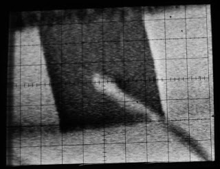
 The next problem I found was apparent at higher magnifications. This photo shows a close-up of one of the chip's bond wire pads. The pad in reality is very straight, but it is quite curvy in this image. At first, I thought this problem was caused by a ground loop between the X/Y amplifier and the rest of the microscope's power supplies. No, it turned out to be caused by the oscillating magnetic field created by the diffusion pump's cooling fan and the pump's heater.
I switched off the pump and fan, and the problem went away. I thought about adding magnetic shielding to the chamber, but I think I will just accept with the wavy image while focusing/panning, then turn off the pump to record an image.
My SEM design is ideal for teaching and exploring electron beam control, but has several major design flaws, which I will summarize for those interested in creating homebrew SEMs with actual utility value:
1. The photomultiplier tube is extremely sensitive to ambient light. In my SEM, I use a black plastic light-tight box to cover the glass bell jar and keep it protected from room lighting. However, the SEM's own filament produces enough light that escapes through the electron gun's vent holes to cause big problems. I can only run the photomultiplier tube at about 700V, before exceeding the average maximum rated anode current (.1mA). The SEM imaging system is AC coupled so the offset is not a deal-breaker, but I believe the DC offset also creates a lot of AC noise in the output image, and would also damage the photomultiplier if I should run it for a long time or greatly exceed the max average anode current. The solution is to build the microscope column from an opaque material (metal), and arrange the electron gun such that there is no optical path from its vent holes to the specimen chamber of the SEM (like all commercial designs).
2. Remove magnetic disturbances or build the SEM column from a magnetically-shielding material.
3. Use very clean, tightly regulated DC for all supplies involved with the project. This is a sensitive analog system, and it picks up every kind of noise.
4. The main accelerating voltage need not be very high (eg 3KV works fine). Lower-energy electrons are easier to deflect and focus, lowering the requirements for those respective power supplies. So far, I haven't seen any benefit to using higher accelerating voltages.
5. Minimize the use of all insulators inside the chamber. Try to build structures that stand on their own without insulator support, or shadow insulators from the electron beam with conductive surfaces. I will talk about this more in a future video, but it caused me many problems in the early weeks of the electron column design.
My next actions will target the overall softness of the image. A youtube commenter pointed out that my aperture disc is much too thick (.010" thick, with a 100um hole). In the pinhole photography world, this would be considered a silly setup and would lead to soft images. I am inclined to believe a similar thing is happening with the electron beam, and will try the same aperture size with a thinner sheet.
I will also try to reduce the amount of light coming out of the electron gun and/or reduce the amount of light entering the photomultiplier. This should reduce the grainy high-frequency noise in the image.
PS, I also think that all of my images are inverted with respect to the normal secondary-electron images from SEMs. All of the images that I have posted so far have dark regions where secondary emission was high. I will probably correct this by adding another inverting opamp the signal chain.

 Here is a shot of the aluminum window screen that I have been using as a test target. The wires in the target are pretty straight, indicating that the system is relatively linear, and can produce an undistorted image.
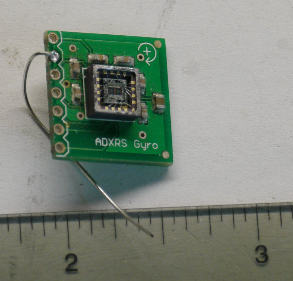
 This photo shows an integrated circuit -- this one is a MEMs gyroscope. The wild black/white pattern on the hard-edged object at lower right is the actual silicon die. I imagine the strange pattern is caused by the varying conductivity of the die's surface. The die's bond wires can be seen clearly as well as the metal pads that connect the bond wires to the chip's external leads.
I spent a good part of the day redesigning my filament power supply. It is now DC and fully regulated. The original design was AC, which caused huge focus problems (the beam would fluctuate at 60Hz, so I rectified it to unregulated DC. Later, I found that the ripple in the output voltage was also causing image problems. Since my image scan rate is on the order of 30Hz (in vertical), I would see the problems caused by 60Hz noise as rolling bars in the output image. The ripple in the DC filament voltage caused strange black bands to roll down the video image. I suspect this happened because of slight changes in the electron gun's bias. I am really surprised that the 2V filament voltage would have any effect on the bias voltage of hundreds of volts, but it apparently does.
 The next problem I found was apparent at higher magnifications. This photo shows a close-up of one of the chip's bond wire pads. The pad in reality is very straight, but it is quite curvy in this image. At first, I thought this problem was caused by a ground loop between the X/Y amplifier and the rest of the microscope's power supplies. No, it turned out to be caused by the oscillating magnetic field created by the diffusion pump's cooling fan and the pump's heater.
I switched off the pump and fan, and the problem went away. I thought about adding magnetic shielding to the chamber, but I think I will just accept with the wavy image while focusing/panning, then turn off the pump to record an image.
My SEM design is ideal for teaching and exploring electron beam control, but has several major design flaws, which I will summarize for those interested in creating homebrew SEMs with actual utility value:
1. The photomultiplier tube is extremely sensitive to ambient light. In my SEM, I use a black plastic light-tight box to cover the glass bell jar and keep it protected from room lighting. However, the SEM's own filament produces enough light that escapes through the electron gun's vent holes to cause big problems. I can only run the photomultiplier tube at about 700V, before exceeding the average maximum rated anode current (.1mA). The SEM imaging system is AC coupled so the offset is not a deal-breaker, but I believe the DC offset also creates a lot of AC noise in the output image, and would also damage the photomultiplier if I should run it for a long time or greatly exceed the max average anode current. The solution is to build the microscope column from an opaque material (metal), and arrange the electron gun such that there is no optical path from its vent holes to the specimen chamber of the SEM (like all commercial designs).
2. Remove magnetic disturbances or build the SEM column from a magnetically-shielding material.
3. Use very clean, tightly regulated DC for all supplies involved with the project. This is a sensitive analog system, and it picks up every kind of noise.
4. The main accelerating voltage need not be very high (eg 3KV works fine). Lower-energy electrons are easier to deflect and focus, lowering the requirements for those respective power supplies. So far, I haven't seen any benefit to using higher accelerating voltages.
5. Minimize the use of all insulators inside the chamber. Try to build structures that stand on their own without insulator support, or shadow insulators from the electron beam with conductive surfaces. I will talk about this more in a future video, but it caused me many problems in the early weeks of the electron column design.
My next actions will target the overall softness of the image. A youtube commenter pointed out that my aperture disc is much too thick (.010" thick, with a 100um hole). In the pinhole photography world, this would be considered a silly setup and would lead to soft images. I am inclined to believe a similar thing is happening with the electron beam, and will try the same aperture size with a thinner sheet.
I will also try to reduce the amount of light coming out of the electron gun and/or reduce the amount of light entering the photomultiplier. This should reduce the grainy high-frequency noise in the image.
PS, I also think that all of my images are inverted with respect to the normal secondary-electron images from SEMs. All of the images that I have posted so far have dark regions where secondary emission was high. I will probably correct this by adding another inverting opamp the signal chain.
Subscribe to:
Posts (Atom)